
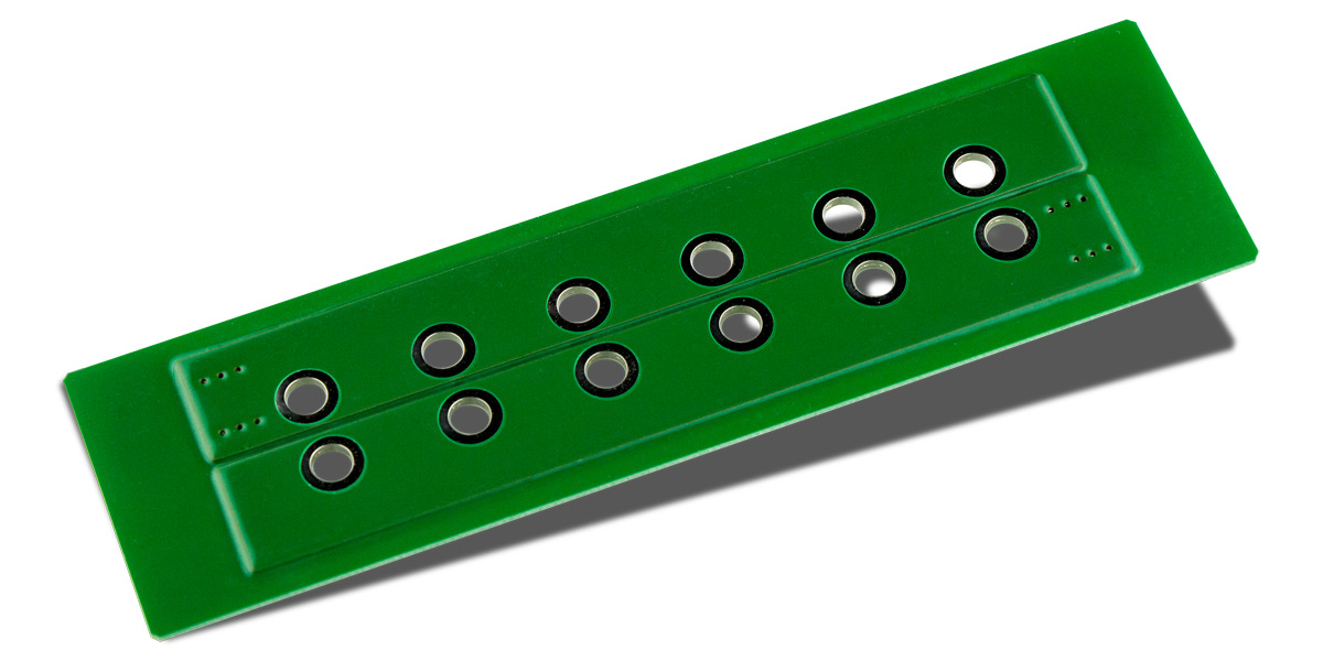
Copper IMS PCB | Printed Circuit Board
Copper IMS PCB Printed Circuit Board
Is the aluminum already 'burning'? No idea where to dissipate the heat? Often, upgrading to copper IMS circuit boards is the only option left.
This opens up a spectrum of many new possibilities: higher thermal conductivity, electrical interconnection between the circuit pattern and the copper carrier, and solderability of the base carrier can represent significant advantages.
Thanks to the extensively tested and reliable composite between copper in general and insulation layers (prepregs) in printed circuit board (PCB) production, very stable and customized special configurations can also be realized here, where the IMS copper can be positioned flexibly or chosen in terms of thickness.


Options |
|---|
| Material properties | 1,0 - 3,0 W/mK, 38 - 100µm isolation |
| Material manufacturers | Bergquist, Ventec und house brands |
| Material thicknesses | 0,8 / 1,0 / 1,6 / 2,0 mm |
| Maximum PCB size | 428 x 568 mm², over-sized IMS-Cu-PCB on enquiry |
| Copper thicknesses | 35µm / 70µm |
| Layer count | 1 to 2 layers |
| Surface finishes | ENIG (immersion gold) |
| Mechanical machining | routing, v-cut/scoring, jump-scoring, countersink-holes |
| Drill options | isolated drills, plated blind vias |
| Metallizations | into the copper carrier possible |
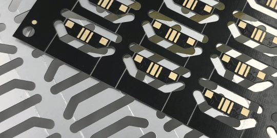
| Solder mask | Lacquer, high reflection lacquer, coverlay Coverlay-colors: yellow, white, black Lacquer-colors: green, yellow, white, black, special colors, matt-lacquers |
| Special prints | Silk print, peelable mask, carbon print |
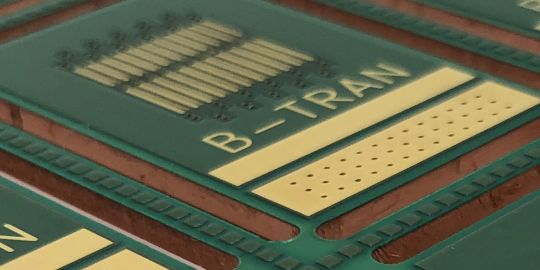
| Special technologies | Multilayer copper-IMS as carrier- and core-types, contacting copper layer with copper carrier (e.g. by plated blind vias) |
| Quality Management & Certifications | ISO 9001, ISO 14001, UL, IPC2/IPC3, IATF 16949, EMPB, VDA2, PPAP, cross-sections, measurement reports, certificate of conformity, data sheets, ESD-packing and more |
| Logistics | Frame-orders, consignment warehouse, call-orders, Sea-air-split-orders |
Definition: Copper IMS PCB
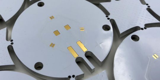
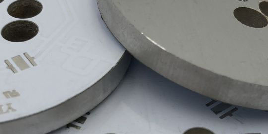
IMS stands for "Insulated Metal Substrate." PCB stands for "Printed Circuit Board." In this context, the conductive copper layer of the circuit board is insulated from the thicker copper of the metal carrier. The insulation layers are usually 50 to 100µm thick. The total thickness of a copper IMS circuit board is typically 1.0mm or 1.6mm, although other thicknesses are available. The copper layer for the electronics is 35µm or 70µm thick, with thicker copper layers sometimes being possible.
Advantages of IMS copper printed circuit boards
Copper IMS PCBs offer advantages when it comes to thermal management:
- Very high thermal conductivity of copper (approximately 380W/mK)/li>
- Very good possibility for contact (e.g., heat-sink via holes in the metal carrier)/li>
- Excellent adhesion in multilayer constructions/li>
- Excellent soldering properties (carrier can be soldered)/li>
However, these advantages are counterbalanced by certain disadvantages. For one, copper IMS circuit boards are very heavy. Additionally, they are significantly more expensive than FR4 or aluminum IMS circuit boards (approximately 5-10 times the cost).
Applications of copper-coated IMS PCB
Due to the significantly higher costs of copper IMS circuit boards compared to aluminum IMS boards, they are actually only considered when either the heat conductivity of the used aluminum is insufficient or it is technically necessary to electrically connect the copper carrier. While this is not possible with aluminum, for instance, you can drill blind holes into the copper carrier and then establish through-hole connections, thereby electrically linking them.
Types of IMS printed circuit boards
Most IMS circuit boards typically have aluminum as the metal carrier, while copper is relatively rare in comparison. In extremely rare cases, entirely different metals such as stainless steel are also used.
Copper PCB characteristics
Aluminium PCB characteristics
The production of our printed circuit boards
Single-layer copper boards follow the manufacturing process of regular FR4 circuit boards unless component holes are needed. Such holes must be pre-drilled larger in advance, insulated with paste, and then re-drilled to the required size into the cured insulation paste to prevent short circuits to the copper carrier. When producing 2-layer copper IMS boards with copper as the core (center), the pure copper core is initially pre-drilled, holes are insulated with paste, and then copper layers are laminated with insulating prepregs. Subsequently, the manufacturing process resembles that of a regular 2-layer circuit board.
Buy affordable copper IMS PCB online directly from manufacturer
Easily and conveniently calculate and order copper IMS circuit boards at fair prices through our online calculation, or inquire via email, and we will provide you with an attractive offer. We are also happy to provide you with comprehensive advice on this topic. (LINK TO CONTACT)
IMS-PCB stands for "Insulated Metal Substrate Printed Circuit Board," and therefore, it is a printed circuit board with a metal substrate (copper or aluminum) that is insulated from the electronic circuit on top. IMS PCBs are often used for applications where efficient heat dissipation is required, as the metal substrate conducts heat better than conventional substrates like FR4. This makes IMS PCBs particularly suitable for power electronics, LED lighting, automotive applications, and other fields where thermal management plays a crucial role. The choice between aluminum IMS and copper IMS depends on the specific requirements of the application, as both materials have different thermal conductivity and costs.
Conventional circuit boards use a material known as FR4 as a base, which consists of a non-conductive epoxy resin and fiberglass mixture. This base material allows for the fabrication of holes, for instance, which can be directly plated through (THP). In contrast, IMS circuit boards use a metal substrate (aluminum or copper) as the base material. Consequently, component holes cannot simply be drilled into this material; they need to be insulated with a paste. A common property mentioned for IMS circuit boards is the thermal conductivity in W/mK (watts per meter x Kelvin). This value pertains not to the thermal conductivity of the metal substrate, but rather to the insulating layer between the copper layer, which serves the electrical function.
An advantage of copper IMS circuit boards compared to aluminum IMS circuit boards lies, firstly, in their higher thermal conductivity (copper ~380W/mK versus aluminum ~240W/mK). Another benefit is the possibility to electrically contact the base copper with plated-through holes. Additionally, the copper base can be surface-finished with methods like ENIG (Electroless Nickel Immersion Gold), which is not feasible with aluminum. However, copper IMS circuit boards have disadvantages such as significantly higher weight (copper 9g/cm³ versus aluminum 2.8g/cm³) and higher cost (6 to 10 times more expensive).
Advantages of Copper IMS Boards:
- Copper as a heat conductor
- Various total thicknesses from 0.8 to 2.0 mm available
- Copper layers of 35µm or 70µm
- Insulation layer thickness of 38 to 100µm
- Thermal conductivity ~380W/mK
- Good chemical contact capability (chemical gold plating of the base possible)
- Copper base also easily solderable
Disadvantages of Copper IMS Boards:
- Very heavy material (specific weight 9g/cm²)
- Very expensive material (6 to 10 times more expensive than aluminum IMS)
IMS circuit boards primarily assist by dissipating heat from electronic components, thus reducing thermal stress. This lower heat exposure generally results in significantly extended lifespans for components, enhancing the overall reliability and failure resistance of the electronics. The advantage of metals like aluminum or copper is also that their excellent thermal conductivity ensures the even distribution and dissipation of localized heat ("hot spots") from heat-emitting components directly into the substrate. Additional cooling methods can be incorporated to enhance the effect of heat dissipation into the metal substrate of the circuit board. This can involve attaching additional passive heat sinks onto the metal substrate and/or employing active cooling of the substrate through fans, or even liquid cooling methods such as water cooling or other fluids, if necessary.
IMS circuit boards should be considered when there is significant heat generation from specific components (e.g., high-power LEDs). This heat can be detrimental to the lifespan of these components, and IMS boards aid in efficiently diverting this heat away from hotspots. However, using IMS circuit boards typically requires a relatively straightforward, preferably single-layer design/layout, as multi-layer IMS boards can quickly become expensive.
The most visually illustrative testing method for verifying heat distribution in electronic assemblies is achievable through the use of thermal imaging cameras. However, these cameras are expensive and not always readily accessible. In the absence of a thermal imaging camera, temperature measurements can be taken using thermometers and affixed temperature sensors, or laser thermometers can be employed to approximate heat distribution. Both approaches are considerably less accurate than thermal imaging, yet they serve as cost-effective alternatives to gain a general understanding of the cooling effect of the IMS circuit board.
To calculate the heat generation from high currents on circuit boards, LeitOn provides a simple online tool. With parameters such as "trace width," "copper thickness," and "current magnitude," this tool can calculate the increase in temperature. Conversely, if the desired maximum temperature increase is provided, the tool can determine the necessary trace width based on the current. You can download the results as a PDF document, containg the heat-chart.
IMS circuit boards with aluminum as the substrate are very commonly used. As a result, there are numerous providers offering cost-effective IMS boards. However, it's important to consider the type of base material used. Inexpensive providers often utilize materials with a very low thermal conductivity for the insulation layer (prepreg), often as low as 1.0W/mK. In its affordable aluminum IMS online calculator, LeitOn offers prepregs starting from 1.5W/mK, featuring various thermal conductivity values up to high-performance prepregs with 12.0W/mK.
Furthermore, LeitOn also offers copper IMS circuit boards in their online calculator. However, copper IMS PCBs are notably more expensive than aluminum counterparts.
Even with IMS circuit boards, it's important not to overlook the current-carrying capacity of the traces. LeitOn provides a free tool for calculating trace heating. Although IMS circuit boards inherently enhance heat dissipation, the heating within the traces significantly influences the choice of copper thickness (35µm, 70µm, or even 105µm). In addition to the overall thickness, determined by the electronic assembly's installation situation, when selecting the insulation layer (prepreg) between the metal substrate and the traces, it's crucial to balance whether a very thin layer with good thermal conductivity can also withstand potential voltage breakdown. We are happy to provide guidance on this matter!
The first step towards reducing critical heat on circuit boards is to increase the copper diameter of the current-carrying traces. If the layout permits, traces should be designed as wide as possible, and copper pour areas should be incorporated wherever feasible. If this isn't sufficient, the copper layer thickness can be increased. Often, the heat generation of the electrical circuit can be brought down to a normal level by increasing the standard 35µm copper thickness to 70µm or 105µm. Additional options include so-called heat sink holes or "thermal vias." This involves adding extra plated-through holes in critical areas that then dissipate heat through their copper walls to another usually opposite external layer.
LeitOn provides a practical online tool for calculating the heat generated by traces in relation to the current. Information about "trace width," "copper thickness," and "current magnitude" is required for the calculation of the temperature rise. It's important to note that the calculated temperature rise should be understood in addition to the ambient temperature. Reverse calculations can also be done by providing the desired maximum additional temperature rise, and the tool calculates the necessary minimum trace width for that purpose. The result can be downloaded as a PDF document with accompanying graphics.
Thermal vias in the context of printed circuit boards are plated-through holes whose purpose isn't to conduct electrical current but rather to dissipate heat. This often requires that a circuit board has at least 2 layers since single-layer circuit boards don't undergo a through-hole process. Multilayer IMS circuit boards come with significantly higher costs. For aluminum IMS PCBs with drilled thermal vias, there's a drawback in that these vias initially need to be isolated from the metal substrate, as copper plating doesn't adhere to aluminum. Such isolation drilling, in turn, reduces the overall aluminum content in the PCB, possibly to the extent that overlapping isolation vias eliminate aluminum entirely from certain areas of the metal substrate. This can even result in the desired effect being reversed to the negative.
Problem of isolation drills in metal substrate (IMS)
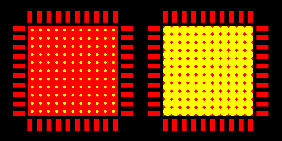
An exception or alternative is represented by so-called thermal blind vias in copper IMS circuit boards. While it is not possible to create through-hole connections with aluminum, this is achievable using copper as the metal substrate. In this case, there's no need to pre-drill larger isolation holes.

since 2021
- CO2 neutral through compensation
- Circuit boards – green on the outside, also on the inside

- Expertise through active exchange
- Expertise through training and further education
- ISO 9001:2015 Quality Management
- ISO 14001:2015 Environmental Management

- UL for rigid FR4 PCBs
- UL for flexible circuit boards
- UL for aluminum IMS boards


