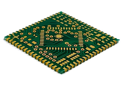
Half-open edges PCBs


The higher level of plated edges is the so called half-open technology for printed circuits. Plated drills are cut in half on the outline of the PCB so that the shape appears like a stamp. Sounds simple but requires multiple additional processes and careful production planning during the CAM layout preparation.

More and more often plated slots, plated edges or even completely plated outlines are required for printed circuit boards. While plated slots are relatively easy to produce, plated slots already require more planning and layout preparation prior to manufacturing. An even higher level of sophistication is reached by half-open printed circuits board edges, where half of the plated drill is cut open.
One may think that half-opens are a simple process flow of drilling, plating and cutting (routing) them in half. However, what will be happening is that the plated copper wall breaks out form the drill due to the horizontal routing force of the routing tool. The copper detaches from the hole before the routing tool is able to cut it. As a consequence, all half-open copper walls will be pressed into the hole from one side.
To avoid the copper walls from collapsing into the plated hole, we change the routing directions and add some processes during CAM preparation. Some production steps are brought forward or done twice. Only such intensive preparation and adjustment of the printed circuit board manufacturing process can assure that half-open PCBs are produced with a flawless stamp-like outline.
For the layout design it is important the minimum drill diameter for half-opens 0,6mm. After halving them only 0,3mm are left. The minimum distance between the annular rings of the half-opens is 0,15mm. Furthermore, we recommend a chemical PCB surface finish such as immersion gold (ENIG or ENEPIG) or immersion tin. HAL lead free may congest the half-opens.
| Characteristics | Values, description |
|---|---|
| material type | FR4 Tg 130°C, FR4 Tg 150°C or FR4 Tg 170°C |
| copper thickness | 35 to 70µm |
| total PCB thickness | 0,5mm to 2,4mm |
| smallest half-open | 0,60mm |
| smallest annular ring for half-open | 0,15mm |
| copper wall thickness of half-open | ca. 20µm |
| surface finishes | immersion nickel-gold (ENIG, ENEPIG) or immersion tin |
| maximum layer count | up to 24 layer multilayer |
| number of outlines with half-opens | 4 (all sides = "stamp") under consideration of break-tabs |


