
Special technologies -
printed circuit boards
printed circuit boards
Versatile special technologies, special types of circuit boards and special processes
Special technologies | printed circuits | PCB | production | multilayer | Flex
Versatile special technologies for printed circuit boards at a glance
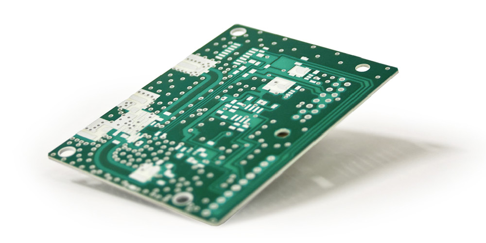
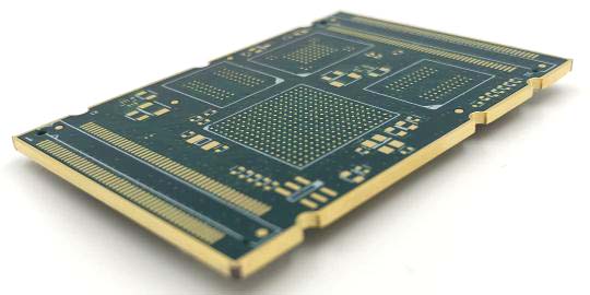
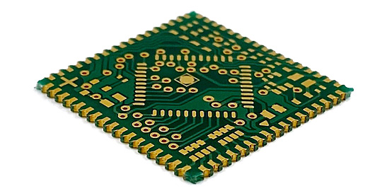
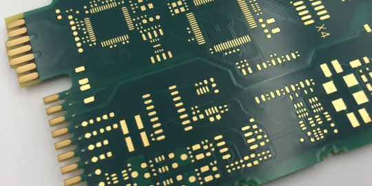
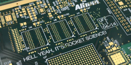
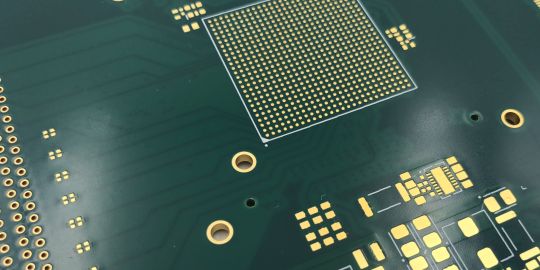
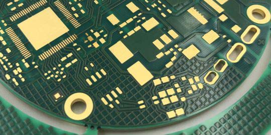
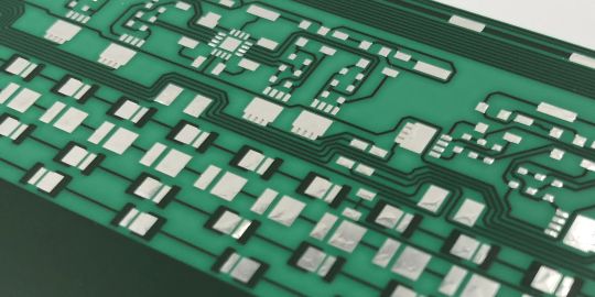
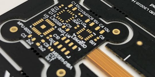
Rigid Printed Circuit Boards (FR4, Rogers, High-TG)
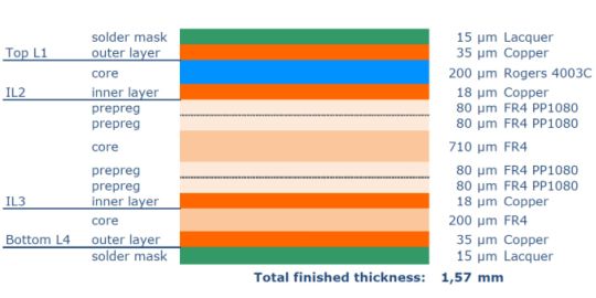
LeitOn GmbH has specialized in cost-effective hybrid solutions that only use expensive RF materials where they are actually needed. The rest remains a conventional FR4 multilayer and therefore cost-effective.
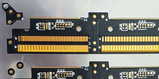
For printed circuits under extreme power conditions, copper thickness of 70µm, 105µm up to 140µm is available for mass production. Prototypes can be produced with copper thickness up to 400µm thick. These copper thicknesses are also available as inner layers so that you can realize solid high-power multilayer-PCB applications.
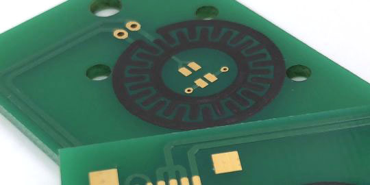
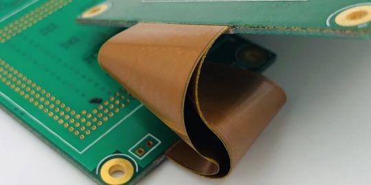
Most FR4 printed circuits can be easily converted into so called semi-flex PCBs. By reducing some areas to a thickness of only 200µm +/-50µm by z-axis routing, these areas become slightly flexible. Flexible enough for so called flex-to-install applications. To avoid solder mask breaking off, a special flex solder mask is applied.
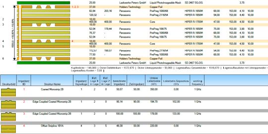
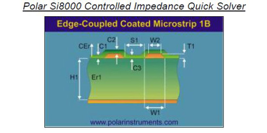
For sensitive high-frequency applications critical impedances can be planned, controlled and measured so that you will only receive PCBs with the requested impedance characteristics. The calculation can be bought from us in advance so that you have all stack-up and material information available early on in your project.
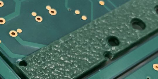
Special routing or milling outlines with toolings down to 0,7mm diameter are common. Usually, such routings are included in the standard price. High tolerance requirements can be incorporated, measured and documented if they are critical to your application. For special purposes we can also use flat-head tools or other equipment.
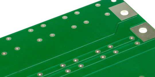
For seamless installation with screws we can add countersink drills into your printed circuit board. Screws will not be visible from the side after installation. Depending on your requirements we can offer a range of different diameters and angles. Please note that additional costs for this countersink process do incur.
If certain areas on the printed circuit must be protected from hot solder wave in some steps, we can cover them with peelable mask on your printed circuit. This peelable mask will protect the area and can be easily removed afterwards. Peelable mask does not leave any residues and the surface underneath remains ready for soldering.
For light-sensitive sensors black solder mask is often not sufficient to block light out. For such requirements we can offer black FR4 material, which is completely opaque and will not let any light diffuse through the PCB. Due to its practical use in the industry it is available for mass production and prototypes.
Keyboards and buttons with partial carbon ink on the PCBs prolong abrasion resistance and are a cost-efficient alternative to hard gold plating. But keep on mind that some design rules must be followed, because the carbon ink is initially liquid when applied and flows slightly on the circuit board before curing.
Standard Rogers 4003C or 4350B materials, and the new 4360G2 are on stock for prototypes and mass production in a wide range of thicknesses. Hybrid stack-ups for multilayers with FR4 and Rogers materials can be produced, too. Impedance measurements at the end of production can assure that the actual printed circuits fulfil your requirements.
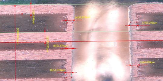
Quality assurance is one thing, documentation another. We understand the need for certainty and can offer extensive documentation of a wide range of individual measurements, according to your needs. Apart from cross-sections and initial sample inspection and impedance reports we can measure individual tolerance requirements.
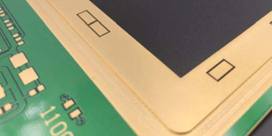
Hard gold thicknesses of 0,5µm to 0,8µm are common for mass production, for prototypes we can produce up to 3µm hard gold. Gold prices can become a real cost driver here. We happily consult you on the application requirements and accompany you with some evaluation cycles in order to determine the optimum gold thickness.
Plated outlines for printed circuit boards are possible. You can partially plate outlines or even almost the entire PCB, so that after separation only the panel connections have no plating. Plated outlines usually require small surcharges, while plated slots, which are located somewhere within the PCB area, are commonly included in the price.
For contacting your printed circuits from the sides we can offer half-open PTH drills. Production of this type of PCB looks simple but it is not. Because simply milling through the PTH at the end of the process would destroy all copper walls, the process involves several mechanical drilling and routing steps around the actual plating process.
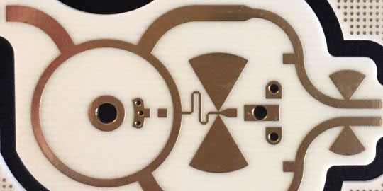
Z-axis milling on PCBs can be produced in a range of widths and depths. Milling can be done as channels or even complete areas can be "lowered" down. Depending on the requirement we can use normal tools or flat-head milling tools which will provide a more even/flat surface, just like semi-flexible printed circuits are produced.
High-TG PCBs with TGs of 150°C, 170°C or even up to 260°C can be offered in a wide range of thicknesses and copper weights. Apart from the obvious advantage regarding temperature performance, high-TG materials also tend to warp less and are therefore preferred materials when it comes to assembling large and complex PCBs.
Plating the z-axis milling with copper on the printed circuit board is also possible. You may for example solder a flange into such a milled and plated z-axis or protect contact areas better. We successfully produced hard-gold-plated z-axis areas to move abrasive contacts below the PCB Top-layer surface level.
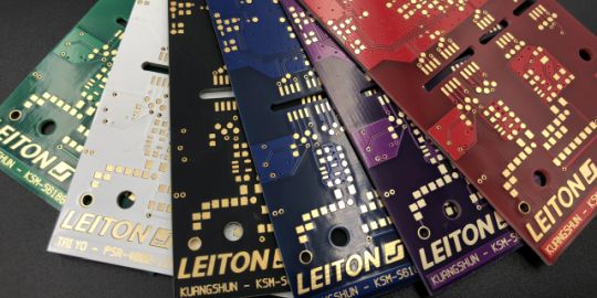
Today red, blue and purple are as common as green, white or black. Many colors are available in matt. If you like to create your own color, keep in mind that such individual colors require minimum order quantities and are therefore often only economically viable for larger quantities. We do keep a wide range of different solder mask color PCBs, ask us for samples.
Regardless of any later impedance measurement or if you prefer to produce the PCB at another supplier, we do offer you full and professional impedance calculation in advance. We will calculate the stack-up and the required trace width/gap as well as the materials. By doing this early on one can be sure that the actual layout will be producible.
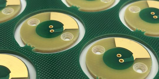
Plugging stands for closing plated through holes and then applying a copper-lid that covers it. You will not only have the hole closed but a copper-pad on top of it which can accommodate a normal soldering process just like any pad. This technology is especially important when the printed circuit board contains BGA components.
Blind vias can be an efficient way to keep the printed circuit board dimensions small. Alternatively, one would have to apply a clearance to these drills in all layers where they do not contact anything and lose this space for routing traces. Although blind vias require a surcharge, it might therefore still be an economically viable choice. If there is even less space, laser vias may be an option.
Connector gold is an electrolytic hard gold with cobalt, which makes the contacts more resistant against abrasive forces. Such hard gold is recommended for connectors with many connection cycles. Additionally, we recommend beveling for smoother connector insertion. Connector gold usually ranges between 0,5µm and 1,2µm hard gold.
SBU stands for Sequential Build-Up and classifies multilayer-PCBs which are not laminated in one single process but consist of several multilayers that are sequentially build together step by step. SBUs are mostly used when vias or blind vias have extreme aspect-ratios which can be made feasible thanks to this SBU process.
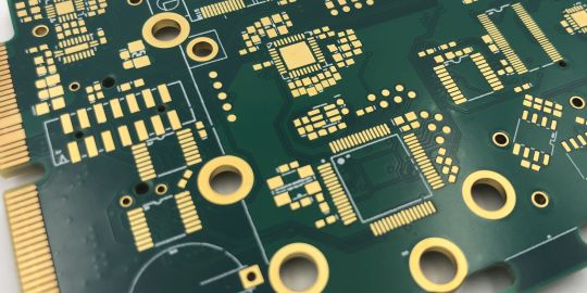
Multilayers with up to 24 layers can be produced as quick-turn prototypes or are available for mass production. Hybrid stack-up, blind vias, 4mil structures, buried vias and copper-lid plugging for BGA components are possible in combination. Usually, such high-layer PCBs are produced with immersion gold finish (ENIG or ENEPIG).
For some applications applying cover-lay onto the PCB is better than solder mask. Usually, cover-lay is only used for flexible circuits. However, we successfully apply cover-lay on some rigid PCBs, too. The advantages are increased abrasive resistance and higher break down voltage resistance. According to IPC solder mask is not allowed as an electric isolator.
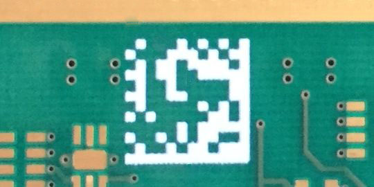
In case each batch or even each single PCB has to be traceable we can accommodate individual IDs on each board or each panel. It is recommended to use DCC codes which are harmonized and can be read by scanners. Depending on the complexity of the required code, such DCC fields only require a small area of the PCB.
Rigid printed circuit boards are available in an almost seamless range of thicknesses, starting at 0,1mm up to 4,0mm. In combination with different copper weights and special material characteristics such as high-TG or CTI, this amounts to an extensive stock of materials that includes hundreds of different material types.
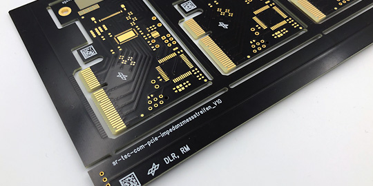
For very tight impedance controlled printed circuit boards measuring one or even several representative coupons of the production panel may not be sufficient. If the exact impedance for each PCB needs to be controlled and be known throughout the entire assembly process we can integrate a test coupon onto the panel.
Special stack-ups can contain a range of deviations from common printed circuit boards. Different materials can be combined in one stack-up (so-called "hybrids") or asymmetric stack-ups can be built. Even different copper thicknesses throughout the PCB are sometimes possible. We can prepare and send you possible stack-ups in advance.
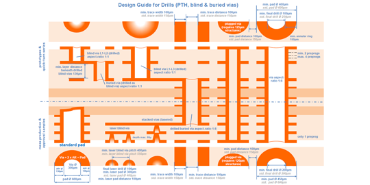
Depending on the country of production, there are different possibilities and restrictions for drilling. For example, laser drilling is not possible everywhere. Mechanical blind holes, on the other hand, also offer their advantages. You can find out what needs to be considered when designing holes by downloading our design guide PDF.
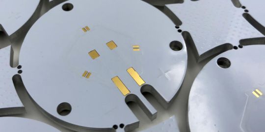
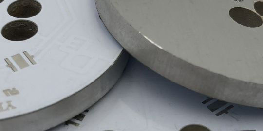
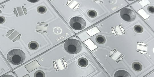
IMS-Printed Circuits (Aluminium/Copper)
In case aluminum IMS printed circuits do not sufficiently cool manage the heat, copper-IMS PCBs are the next step. Copper-IMS PCBs even allow thermo-blind-vias inside the layout which connect them directly to the copper base carrier by plated blind vias. Heat can then directly dissipate into the copper-carrier.
There is a difference between aluminum carrier and aluminum core PCBs. Aluminum carrier PCBs do have the aluminum visible on one side. It "carries" the layout. Aluminum core PCBs have the aluminum in the middle between two or more layers of the layout, so that you can not see the aluminum from one side. Vias are isolated from the aluminum.
For special heat requirements aluminum IMS printed circuits can be produced with materials of a higher heat dissipation of up to 12,0 W/mK. Isolation thickness between aluminum carrier and layout is usually 100µm. Heat management improves significantly, compared to the standard 1,0 to 3,0 W/mK materials.
LED applications which require high light emitting power or better reflections can be produced with a special white high-reflection solder mask. Because light efficiency improves with this solder mask, less expensive LEDs may be used. Taiyo high reflection white solder mask is available for series and mass production.
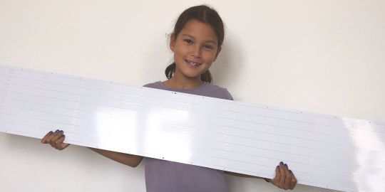
With a total length of 1500mm or 1,5 meters one can create impressive light installations on aluminum-IMS printed circuits that operate with reliable heat management on the backplane. Thanks to the possible length installation becomes easier and cumbersome and risky connectors between several aluminum-IMS PCBs become obsolete.
Instead of white high-reflecting solder mask we can apply special colors like red, blue or black on the aluminum-IMS printed circuits. Nowadays matt-black solder mask is in high demand. Other individual colors can be custom made for your application but are often only economically viable for bigger quantities.
Aluminum-IMS printed circuits can also be produced on thick 4mm carriers. With such a thick base plate one can literally integrate the cooling body into the application. Z-Axis milling on the aluminum side are possible, so that the board can fit into the device and maybe support cooling of adjacent components, too.
Apart from countersinks which are also possible in standard FR4 printed circuits, aluminum materials allow us to insert threads. For smoothly rounded edges punching tools can be used. V-cuts/scoring is also possible for aluminum boards, so you can easily separate the single PCB from its panel after assembly.
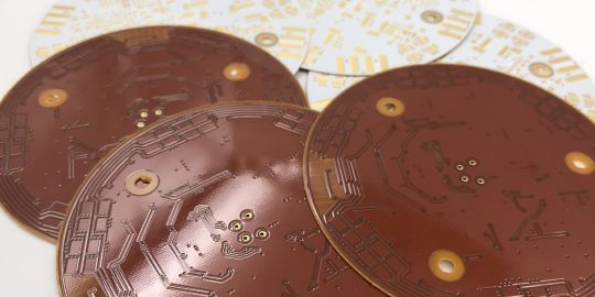
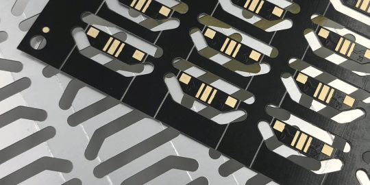
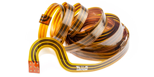
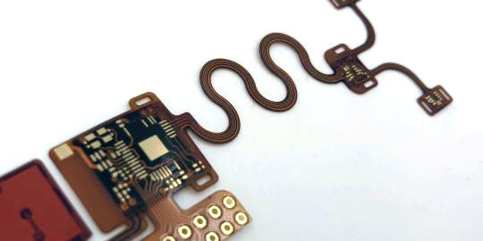
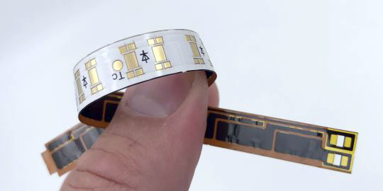
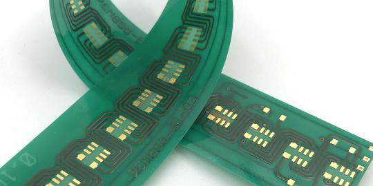
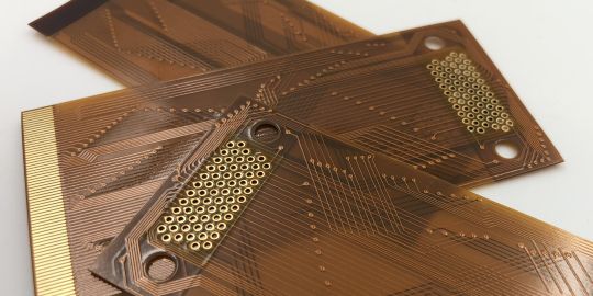
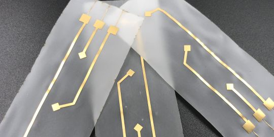
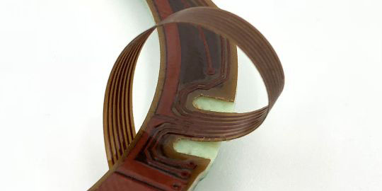
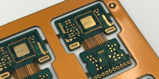
Flexible Printed Circuits (Polyimid/PET)
With a small layout trick you can generate extremely long flexible cables by folding the flexible printed circuit after assembly. The folding points can either be soldered together or we apply some 3M-adhesive. The big advantage is that the costs are of a conventional FPC instead of the high cost reel-to-reel circuit alternative.
Extreme thin (so-called "0mm-slots") or highly complex cuts can be done by laser. Especially when tolerances on the FPC are getting tight, laser cut machines can align the cuts of each critical area separately to achieve higher accuracy. For some connectors we successfully achieve tolerances of only +/-0,05mm.
White cover-lay on your flexible circuits improve light reflection and enhance their appearance. In case you require absolute opacity, black cover-lay will do the job. High dynamic bending is still possible with white cover-lay as there is no wet mask (solder mask lacquer) applied on the circuits. For mass production costs are usually similar like standard yellow/brown cover-lay.
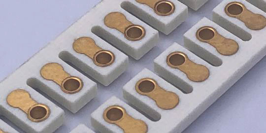
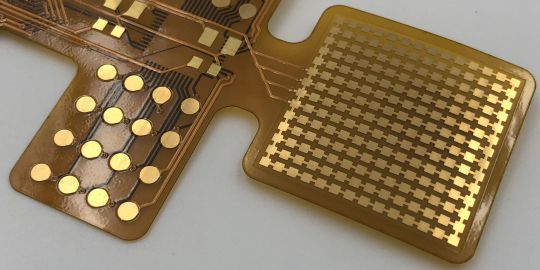
Certain contacting mechanics require physical elevations on the FPC. For such applications we can use a special tooling and punch dimples into the pads so that these are elevated and can be contacted easily. A famous example where this technology is used in household products are inkjet printing cartridges.
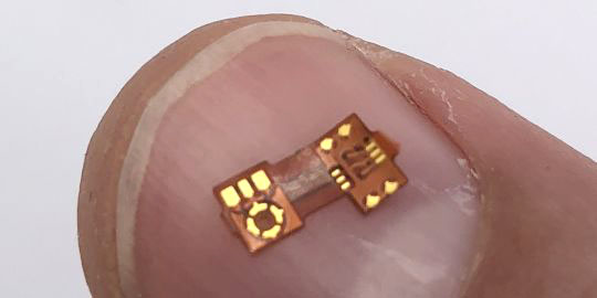
Devices are becoming smaller and smaller. Flexible circuits cannot only be extremely thin but thanks to laser-cut or punching, extremely small in size. FPCs with dimensions of less than 2mm are common in many applications today. The real challenge comes with FPC assembly of such micro-sized circuits.
Apart from ZIF/LIF connectors with 0,3mm polyimide stiffeners we can produce any shape, any thickness and almost any material and attach it as stiffeners: polyimide, FR4 and even stainless steel are possible. You can shield areas or support solder pads of components and prevent them from breaking in a dynamic bending application.
Automatic assembly of flexible circuits can be a real hassle. FPCs tend to bend and fold, which makes component placing difficult to sometime even impossible. We offer a solution by FPC-fixtures which hold your FPC plane and stable during assembly. You can then use automatic loaders by inserting these trays.
Full flexibility is not always an advantage. Sometimes it is just enough to bend the circuits a little bit instead of fold. Here we can offer 0,1 - 0,2 mm FR4 materials. Production process is easier than for flexible printed circuits, for example because wet flexible solder mask can be used. Economically it is worth considering before going for FPCs.
If you do not want to use FPC fixtures for assembly we can attach the flexible circuits on FR4 carriers by using reflwo-resistant tape on the sides. The FPCs can then be assembled almost as good as within the fixture but the costs per piece will be higher. For medium quantities, this may be the best alternative.
You can design your PCBs with partial or full areas of 3M adhesive. After removing the liner, the 3M adhesive on your FPC allows you to exactly position and fix the circuits inside your application. Reflow-oven resistant 3M adhesives are available so you can solder them just like any other flexible circuit.
Flexible multilayers up to 6 layers can be produced as prototypes or series/mass production. For flexible circuits, uneven layer counts like 3 or 5 layers are common and can be produced. Instead of conventional fiber-glass prepregs, such FPC multilayers use epoxy or acrylic adhesive sheets for lamination.
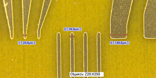
Trace/gap structures down to 1mil (0,025mm) are possible for flexible printed circuits. Such extremely thin traces can also enhance the dynamic bending performance because less copper is there to inhibit the bending. However, 2mil trace/gap does come with a higher price than conventional structures.
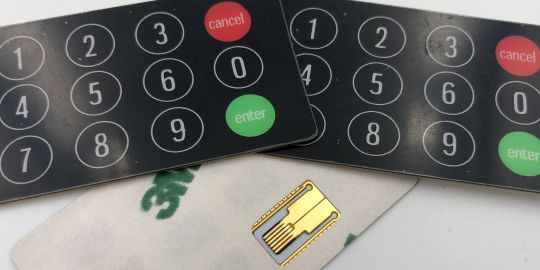
One next step for flexible circuits are so called keypads. Small metal domes are added to give a pressure feedback. Then a printed cover is added with the position of the buttons and other information. The backside has the gold plated connector and optional 3M adhesive for easy installation in the application.
Ultra-thin flexible polyimide films with only 13µm material thickness plus copper allow extreme bending radiuses. For such single layer FPCs with only 12µm copper thickness, without solder mask or cover-lay, you can achieve a total thickness of only 0,025mm (25µm) for an electrically functioning printed circuit foil.
Almost transparent FPCs can be produced by using PET (Polyethylenterephthalate) instead of PI (polyimide). Such material - in combination with silver ink print - is cheaper in mass production, but such applications are almost extinct in Europe. Today it is mostly different material requirements which make PET with copper a favorable alternative.
Flexible printed circuits can also be produced with hard gold. Common hard gold thicknesses range from 0,5µm to 0,8µm, sometimes up to 1,2µm. If possible, the pads receiving hard gold should be located on the edge of the FPC, so it can be connected to a plating bus. If this is not possible, the more complex etch-back process comes into play.
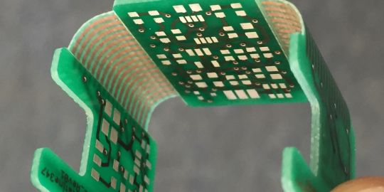
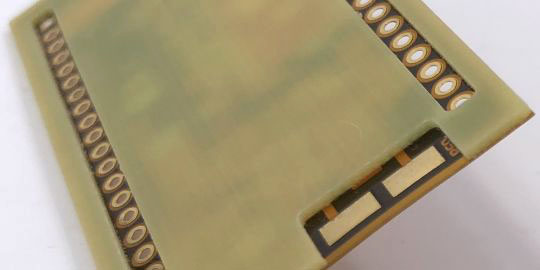
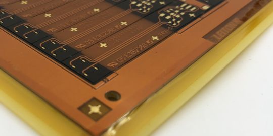
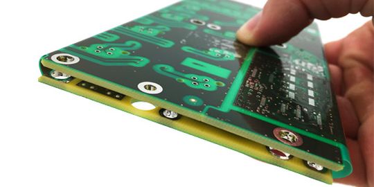
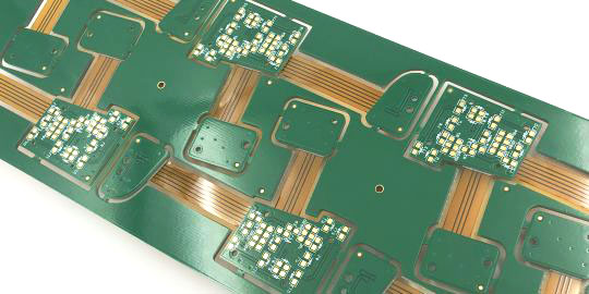
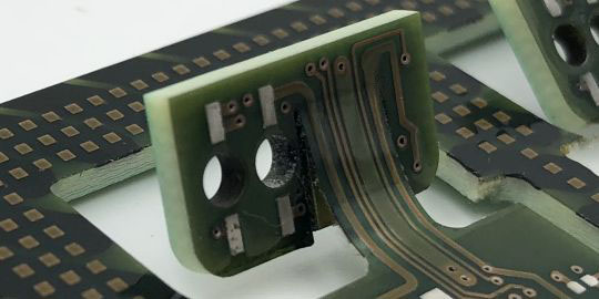
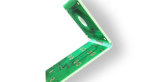
Rigid-Flexible Printed Circuits (RFPCB)
The cryptic classification of rigid-flexible stack-ups like "2LA1" comes from a simple logic. The first number with the letter "L" tells us the total layer count. The "A" stands for the German word "außen" (engl. "outer"), which is the position of the flex layer. Finally, the last number tells us the quantity of the flex layers. Some call a 4LI2 ("I" for "inner") 1R+2F+1R.
Rigid-flexible PCBs are much easier handled inside a panel, so that the flexible areas do not bend during assembly. Additionally, panels protect the RFPCB during shipment and transportation. We can help setting up your custom-panel design, optimized for your assembly process as well as for maximum panel utilization to safe costs.
For 3- or 4-layer rigid-flexible PCBs the flexible layers can be moved to the inner layers. Due to this layer position dynamic bending performance in both directions improves significantly. 4LI2 is standing for a 4-layer RFPCB with 2 inner flexible layers. With flexible layers on the outside, it would be called 4LA2 ("A" for "außen", english "outer").
Bookbinder-technique is used when more than 2 flexible inner layers are required to maintain a maximum degree of bendability. All flexible layers are on top of each other but not glued/laminated together. If all flex layers would be laminated together, flexibility of this rigid-flexible board would decrease significantly.
Lift-off-areas are areas in the rigid area where there is no adhesive used to attach the flexible parts. This allows bending within the rigid dimensions, not having to add any space for the bending radius itself. Rigid-flexible PCBs can therefore be even more efficiently used in devices with limited space.
In case the layout is packed and there is not enough space for normal lift-off-areas a laser-cut can be used. However, as the laser inevitably burns into the underlying FR4, residues may be visible. For the bending application one should also consider that such thin cuts can tear into the flexible area.
For pure FR4 rigid-flexible PCBs the flexible polyimide part is replaced by a very thin FR4 core. This core is also flexible but because the process does not require milling the core like with conventional semi-flex, the bending performance is much better. Costs are usually slightly lower than for conventional rigid-flex with polyimide flex-layers.
Rigid-flexible PCBs can also be produced with blind vias or buried vias. However, plugging is sometimes only possible if the flexible layers are in the inner layers or if a pure FR4 rigid-flex is being chosen. The reason is the necessary polishing step after plugging, for which polyimide-based laminates are not applicable.

Climate-neutral operation
since 2021
since 2021
- CO2 neutral through compensation
- Circuit boards – green on the outside, also on the inside

Member of the Fachverband Elektronik-Design
- Expertise through active exchange
- Expertise through training and further education
ISO tested by the most renowned auditor in Germany
- ISO 9001:2015 Quality Management
- ISO 14001:2015 Environmental Management

UL approvals for various types of circuit boards
- UL for rigid FR4 PCBs
- UL for flexible circuit boards
- UL for aluminum IMS boards


